- 您现在的位置:买卖IC网 > Sheet目录1998 > ICS844002AG-01LF (IDT, Integrated Device Technology Inc)IC SYNTHESIZER 2LVDS 20-TSSOP
ICS844002-01
FEMTOCLOCKS CRYSTAL-TO-LVDS FREQUENCY SYNTHESIZER
IDT / ICS LVDS FREQUENCY SYNTHESIZER
2
ICS844002AG-01 REV. A SEPTEMBER 28, 2007
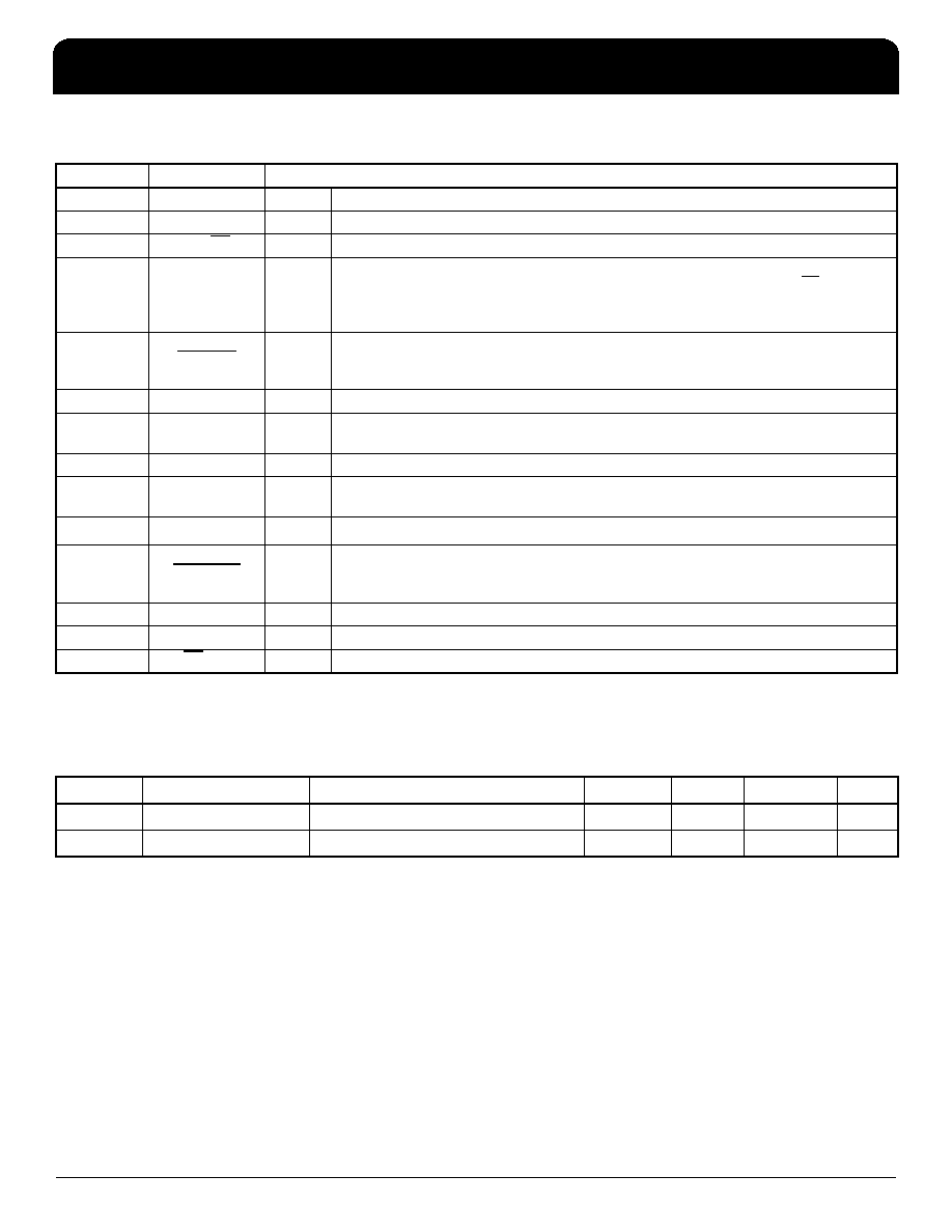
Table 1. Pin Descriptions
NOTE: Pulldown refers to internal input resistors. See Table 2, Pin Characteristics, for typical values.
Table 2. Pin Characteristics
Number
Name
Type
Description
1, 7
nc
Unused
No connect.
2, 20
VDDO
Power
Output supply pins.
3, 4
Q0, Q0
Output
Differential output pair. LVDS interface levels.
5
MR
Input
Pulldown
Active HIGH Master Reset. When logic HIGH, the internal dividers are reset
causing the true outputs Qx to go low and the inverted outputs Qx to go high.
When logic LOW, the internal dividers and the outputs are enabled.
LVCMOS/LVTTL interface levels.
6
PLL_SEL
Input
Pulldown
Selects between the PLL and REF_CLK as input to the dividers. When LOW,
selects PLL (PLL Enable). When HIGH, deselects the reference clock (PLL
Bypass). LVCMOS/LVTTL interface levels.
8VDDA
Power
Analog supply pin.
9,
11
FSEL0,
F_SEL1
Input
Pulldown
Frequency select pins. LVCMOS/LVTTL interface levels.
10
VDD
Power
Core supply pins.
12,
13
XTAL_OUT,
XTAL_IN
Input
Parallel resonant crystal interface. XTAL_OUT is the output,
XTAL_IN is the input.
14
REF_CLK
Input
Pulldown
Non-inverting differential clock input.
15
XTAL_SEL
Input
Pulldown
Selects between crystal or REF_CLK inputs as the PLL Reference source.
Selects XTAL inputs when LOW. Selects REF_CLK when HIGH.
LVCMOS/LVTTL interface levels.
16
nc
Unused
No connect.
17
GND
Power
Power supply ground.
18, 19
Q1, Q1
Output
Differential output pair. LVDS interface levels.
Symbol
Parameter
Test Conditions
Minimum
Typical
Maximum
Units
CIN
Input Capacitance
4
pF
RPULLDOWN Input Pulldown Resistor
51
k
发布紧急采购,3分钟左右您将得到回复。
相关PDF资料
ICS844002AGI-01LFT
IC SYNTHESIZER 2LVDS 20-TSSOP
ICS844002AGLF
IC SYNTHESIZER 2LVDS 20-TSSOP
ICS844004AK-104LF
IC SYNTHESIZER LVDS 32-VFQFPN
ICS844004AKI-104LFT
IC SYNTHESIZER LVDS 32-VFQFPN
ICS844021BG-01LFT
IC CLOCK GEN ETHERNET 8-TSSOP
ICS844021BGI-01LFT
IC CLOCK GEN ETHERNET 8-TSSOP
ICS844071AGLFT
IC CLOCK GEN GIG ETH 8-TSSOP
ICS844201BG-45LF
IC CLK GENERATOR 25MHZ 8TSSOP
相关代理商/技术参数
ICS844002AG-01LFT
功能描述:IC SYNTHESIZER 2LVDS 20-TSSOP RoHS:是 类别:集成电路 (IC) >> 时钟/计时 - 时钟发生器,PLL,频率合成器 系列:HiPerClockS™, FemtoClock™ 标准包装:1,000 系列:- 类型:时钟/频率合成器,扇出分配 PLL:- 输入:- 输出:- 电路数:- 比率 - 输入:输出:- 差分 - 输入:输出:- 频率 - 最大:- 除法器/乘法器:- 电源电压:- 工作温度:- 安装类型:表面贴装 封装/外壳:56-VFQFN 裸露焊盘 供应商设备封装:56-VFQFP-EP(8x8) 包装:带卷 (TR) 其它名称:844S012AKI-01LFT
ICS844002AGI-01LF
功能描述:IC SYNTHESIZER 2LVDS 20-TSSOP RoHS:是 类别:集成电路 (IC) >> 时钟/计时 - 时钟发生器,PLL,频率合成器 系列:HiPerClockS™, FemtoClock™ 标准包装:1,000 系列:Precision Edge® 类型:时钟/频率合成器 PLL:无 输入:CML,PECL 输出:CML 电路数:1 比率 - 输入:输出:2:1 差分 - 输入:输出:是/是 频率 - 最大:10.7GHz 除法器/乘法器:无/无 电源电压:2.375 V ~ 3.6 V 工作温度:-40°C ~ 85°C 安装类型:表面贴装 封装/外壳:16-VFQFN 裸露焊盘,16-MLF? 供应商设备封装:16-MLF?(3x3) 包装:带卷 (TR) 其它名称:SY58052UMGTRSY58052UMGTR-ND
ICS844002AGI-01LFT
功能描述:IC SYNTHESIZER 2LVDS 20-TSSOP RoHS:是 类别:集成电路 (IC) >> 时钟/计时 - 时钟发生器,PLL,频率合成器 系列:HiPerClockS™, FemtoClock™ 标准包装:1,000 系列:- 类型:时钟/频率合成器,扇出分配 PLL:- 输入:- 输出:- 电路数:- 比率 - 输入:输出:- 差分 - 输入:输出:- 频率 - 最大:- 除法器/乘法器:- 电源电压:- 工作温度:- 安装类型:表面贴装 封装/外壳:56-VFQFN 裸露焊盘 供应商设备封装:56-VFQFP-EP(8x8) 包装:带卷 (TR) 其它名称:844S012AKI-01LFT
ICS844002AGILF
功能描述:IC SYNTHESIZER 2LVDS 20-TSSOP RoHS:是 类别:集成电路 (IC) >> 时钟/计时 - 时钟发生器,PLL,频率合成器 系列:HiPerClockS™, FemtoClock™ 标准包装:27 系列:Precision Edge® 类型:频率合成器 PLL:是 输入:PECL,晶体 输出:PECL 电路数:1 比率 - 输入:输出:1:1 差分 - 输入:输出:无/是 频率 - 最大:800MHz 除法器/乘法器:是/无 电源电压:3.135 V ~ 5.25 V 工作温度:0°C ~ 85°C 安装类型:表面贴装 封装/外壳:28-SOIC(0.295",7.50mm 宽) 供应商设备封装:28-SOIC 包装:管件
ICS844002AGILFT
功能描述:IC SYNTHESIZER 2LVDS 20-TSSOP RoHS:是 类别:集成电路 (IC) >> 时钟/计时 - 时钟发生器,PLL,频率合成器 系列:HiPerClockS™, FemtoClock™ 标准包装:1,000 系列:- 类型:时钟/频率合成器,扇出分配 PLL:- 输入:- 输出:- 电路数:- 比率 - 输入:输出:- 差分 - 输入:输出:- 频率 - 最大:- 除法器/乘法器:- 电源电压:- 工作温度:- 安装类型:表面贴装 封装/外壳:56-VFQFN 裸露焊盘 供应商设备封装:56-VFQFP-EP(8x8) 包装:带卷 (TR) 其它名称:844S012AKI-01LFT
ICS844002AGLF
功能描述:IC SYNTHESIZER 2LVDS 20-TSSOP RoHS:是 类别:集成电路 (IC) >> 时钟/计时 - 时钟发生器,PLL,频率合成器 系列:HiPerClockS™, FemtoClock™ 标准包装:1,000 系列:- 类型:时钟/频率合成器,扇出分配 PLL:- 输入:- 输出:- 电路数:- 比率 - 输入:输出:- 差分 - 输入:输出:- 频率 - 最大:- 除法器/乘法器:- 电源电压:- 工作温度:- 安装类型:表面贴装 封装/外壳:56-VFQFN 裸露焊盘 供应商设备封装:56-VFQFP-EP(8x8) 包装:带卷 (TR) 其它名称:844S012AKI-01LFT
ICS844002AGLFT
功能描述:IC SYNTHESIZER 2LVDS 20-TSSOP RoHS:是 类别:集成电路 (IC) >> 时钟/计时 - 时钟发生器,PLL,频率合成器 系列:HiPerClockS™, FemtoClock™ 标准包装:1,000 系列:- 类型:时钟/频率合成器,扇出分配 PLL:- 输入:- 输出:- 电路数:- 比率 - 输入:输出:- 差分 - 输入:输出:- 频率 - 最大:- 除法器/乘法器:- 电源电压:- 工作温度:- 安装类型:表面贴装 封装/外壳:56-VFQFN 裸露焊盘 供应商设备封装:56-VFQFP-EP(8x8) 包装:带卷 (TR) 其它名称:844S012AKI-01LFT
ICS844002AKLF
功能描述:IC SYNTHESIZER 2LVDS 32-VFQFPN RoHS:是 类别:集成电路 (IC) >> 时钟/计时 - 时钟发生器,PLL,频率合成器 系列:HiPerClockS™, FemtoClock™ 标准包装:1,000 系列:- 类型:时钟/频率合成器,扇出分配 PLL:- 输入:- 输出:- 电路数:- 比率 - 输入:输出:- 差分 - 输入:输出:- 频率 - 最大:- 除法器/乘法器:- 电源电压:- 工作温度:- 安装类型:表面贴装 封装/外壳:56-VFQFN 裸露焊盘 供应商设备封装:56-VFQFP-EP(8x8) 包装:带卷 (TR) 其它名称:844S012AKI-01LFT